Q: I..am having some difficulty with compiling the first program (experi1.c). I am using Visual C++ 6.0 on Windows XP and recieve the error "unresolved symbol _imp" during the linking phase of the build. I have also tried building it under DOS 6.22 using a free compiler named the Pacific C compiler and recieve the error "undefined symbol" with the cursor positioned at the line that contains "((inp(switch_port) >> (input +3))&1 ^1", indicating that this is the line that contains the error.
A: If you read the main page, you will find that it says, among other things that
"The tutorial examples will work on most operating systems that allow direct access to ports (more on ports later). They will not work with NT, 2000, XP or other operating systems that do not permit direct port access. DOS, Win 3.x, Win95, Win98 and WinMe will work, among others."
One of your problems lies in the fact that XP does not permit direct port access.
If you have yet to download Pacific's manual, you need to do so at http://www.htsoft.com/products/pacific.html
Port access is explained on page 72. It's a little confusing with all of the references to assembly code, but just as useful as inp() and outp(). Use the form
port unsigned char io_port @ 0xe0;
from their example. Your port name and location will, of course, be
different:
port unsigned char switch_port @ 0x318;
This would replace the two lines
#define base 0x300 // change if a conflict is found
#define switch_port base + 0x18
and you should be able to remove the inp():
return (switch_port >> ((input + 3) & 1)) ^ 1;
In other words, any time you make reference to switch_port after making the declaration, you actually make reference to the port address and get data from it.
Q: I want to know how to write the test routines in c to apply inputs like voltage to a resistor and measure the current from it.
A: You might try the following:
The resistor should be a value that is significantely lower in value
than any you expect to see in the circuit you are testing. Also, the
board and the circuit you are testing must have the same ground. Above
all, it should never be used in an attempt to measure
AC line current!! Use it for low DC currents only.
Get the inputs for AD1 and AD2 (any two of the 8 AD inputs can be
used). Use C procedures similar to those you can find in Experiment 9 to get the values for each side.
Now find the difference of the two values. This will be related to the
voltage drop across the resistor. Now use Ohm's law to get the current:
I = V/R
Thus, if R = 1 ohm and the drop is .1 volt, the current is .1 amp.
You will need to determine the numerical value your particular converter
returns for a given voltage. Use that ratio as a conversion to determine
voltage rather than the idealized values used in the text.
Q: In Experiment 1, I couldnt figure out how the switch port address was calculated as 0x318.
A: The base address determination is convered on the hardware page
The devices on the board are 8 bytes away from each other, starting with the Analog to Digital Converter (also noted on the hardware page). You might want to re-read the hardware page and the sections dealing with HEX notation as it relates to actual bits on the address and data busses.
Q: In Experiment 2, when you say "Connecting
pin 9 to pin 1 or 25 of Header 3 should indicate that switch 4 has been
turned on." How exactly are we to connect pin 9 to pin1? I mean is this
done physically by means of a jumper etc.?
A: The best way to do this would be with a
ribbon cable similar to the one described in Experiment 1 and included
with Experimenter's Kit #1 found on the order
page. The wires are simply touched together.
Q: I am doing a project in building device
drivers for a ADC and DAC. We [are supposed to] read back the motor
speed through the ADC. The problem is how to convert the mechanical
energy into analog signal? We will use a Frequency to voltage converter.
A: I don't do homework, but I'll give you a
hint. Connect a low-value resistor from one of the motor's terminals to
ground. Use an oscilloscope to look at that terminal while you vary the
voltage to the other terminal.
Q: Please give me a hint about how to read the
motor speed back into the computer through ADC.
A: What did you see when you ran the test I
suggested? If you don't have a scope, try connecting the terminal
through a capacitor to an audio amplifier (this presumes you are using a
good, isolated power supply for the test -- not AC line voltage!!). Now vary the voltage on
the other terminal. Now, what does a FV converter do?
Q: Great tutorial!!
A: Thank you. (not a question, but I
sure like stuff like that!)
Q: On Experiment2 I was wondering where the (active low) CS signal that goes to IC3 8255A pin 6 actually comes from. This incoming signal is labeled (active low) PPI SELECT. I'm trying to figure out all of the necessary signals that are needed to actually write to the control register. I understand that 0x23 in base + 0x23 will set pins 8 and 9 high (A1 and A0, respectively), and the write signal to pin 36 is automatically taken low by the PC when the outp_ function is invoked but I'm not certain what roll the (active low) PPI SELECT plays in the control register setup. Thanks!
A: PPI SELECT comes from the 74LS138 and was actually shown there as the PIO SELECT. PIO means "Peripheral I/O" and is often used interchangeably with PPI, although PIO is more often used with the Motorola peripheral interface chip. I have changed the reference in Figure 1 to make it clearer.
Register select is a combination of address, select and read/write. See the tables in the 8255 data sheet and Experiment 2 for more detail.
Q: Do you know if it is possible to draw a small circle (about the size of a penny) on the screen and link it to an input byte (for exmple: a byte from Experiment1) and change the color (depending on bit status of the desired byte) of this filled circle from red (for off) to green (for on) using C ? I have checked my book "A Book on C" and didn't find anything on the subject and I also checked a few C boards and still had no luck. Can drawing even be done using the C language? Thank you again and again your time is once again appreciated.
A: Go to my Super Start site then to the Free Downloads section. Download the full zip. The test program does something similar to what you are talking about. It first queries the board (after it detects its presence -- I will discuss auto-detect for the board when I get into the analog sections), then prints switch numbers on the screen, with green meaning off, and red meaning on. That section is not graphics though, but colored text.
You can also draw in C, but it depends on the compiler. MIX has one of the best selections I have seen, which is the reason I used it for Super Start -- it uses a lot of graphics.
Q:Does the program actually place the Hex value 0x318 on the Address lines of the ISA Bus in the fashion that I have stated?
A:Everything eventually must get down to high or low bit indications on the bus. The binary is a closer text representative of the pattern on the bus.
Q:How does the PC know that a valid port address has been detected and does the PC actually force the AEN signal to go low when this valid port address has been detected?
A:IN or OUT commands cause the processor to make AEN low and either IOR or IOW low.
Q:Does the program statement
return ((inp(switch_port) >> (input + >3)) & 1) ^ 1;
actually force the IOR (active low) signal to go low?
A:The inp() part does, along with causing AEN to go low and setting up the port address.
Q:Does IC7 74LS244 Pin 19 (EOC/SWITCH SELECT) have to be manually placed low by the user?
A:No. This is a select line from the '138. A switch would have to be taken low by the user (could be a switch or something that looks like one). EOC stands for End of Conversion. It connects to the Analog to Digital Converter and signals the end of an AD conversion.
Q:I'm not sure what purpose IC11 Pin 19 actually surves in this experiment?
A:This line enables IC12 so data can be placed on the data bus in the case of inp(), or placed on a device on the board in the case of outp(). It also activates IC10 which then further decodes the selected address and selects the particular device on the board.
Q:Most importantly I am trying to understand how the PC actually knows that the inputs from Experiment 1 are at port address 0x318. It appears that IC11 74LS688 only compares address lines A6-A9, this would only check to see if DIP SW1-SW3 have been set to 001 which represents Hex value 0x300. How does this relate to the Hex value 0x318 that is addressed in the program?
A:IC 10 does the rest of the decoding.
Q:When an ISA card is used and port addressing is assigned, is it a known that 64 bytes will be consumed by the card, it appears that in all of your examples the range is 64 bytes (200-23f, 300-33f)?
A:Yes, it is known by the user. The computer does not automatically know anything. Being one of the dumbest things on earth ("only knows how to count from 0 to 1" wouldn't look too good on the ol' resume), it knows only what it is told.
Q:The address used in Experiment 1 is port address 0x318, the end result is a possibility of 8 bits (only 3 of which are being used in Experiment 1) being placed directly on the ISA Data bus. The ranges (Experiment 1 uses 0x318-0x31f), when broken down, for all of the experiments each have a decimal value of 8 ( 0-7 ). Is the port address what actually holds the Data Bus values from the ISA card?
A:The data bus will hold values for a length of time specified in the microprocessor data sheet. It is the responsibility of the hardware designer to insure that devices will be able to grab the data in time. The same thing applies to placing data on the bus.
Q: I am working with experiment 4. I have replaced the individual diodes with an inverter which is used to control the Port A lines. I am using a 7414 instead of a 7405. Currently I have a matrix that has the possibility of 24 closures. I am using dip switches as inputs. My control lines are Port A Bits 0,1,2 (rows), and Port B as input (columns). So each Port A bit strobes a row of 8 switches.
When I used individual diodes, the circuit worked properly, meaning that any number of switches that were or were not activated were read correctly by the program.
My problem arose when I replaced the diodes with the inverter. The circuit and program work correctly when any switch or switches within a row are activated. If a switch from another row is activated, the program returns incorrect results. Using a DMM, I have found that during this time, there is a reading of about .245 volts on more than one output line of the 7414.
Do you think that I may have a loading problem, possibly a timing problem, or that a 7414 is just the wrong device for the application. I have considered installing 1) a delay in the code or 2) a driver IC for the outputs of the 7414.
A: The description of the 74LS05 begins: "The 74LS05 (see 74LS05.PDF) and similar devices do not produce a high output. They only pull things low, commonly called sinking, which is what they can do with the pullups on Port B." The fact that the 74LS05 does not produce a high output is its most important characteristic insofar as this application is concerned. A 7414 (see 74LS14.PDF), on the other hand, typically produces about 3.4V, or at least will try to. The low and high outputs can still fight each other if two or more switches are turned on. On the other hand, the 74LS05 can only provide what the pullup resistor provides because it has no circuitry to produce a high output on its own. It has what is called an open collector output. Study the matrix very carefully and imagine devices that can produce high as well as low outputs connected to it. Now imagine two of the switches being turned on with one high and the other low. I think you will see that two of the outputs could be connected to each other. The outputs of devices that can produce both active highs and lows should never be connected to each other.
Q:I was doing experiment 2 as described on your site, using the same code except with base address 0x200. It compiled and ran but it shows that the 8255 inputs are constantly 1. I don't have this problem with the 3 basic switch inputs. I checked the circuit board with an ohmmeter and I get 30 ohms between the I/O posts on header 3 and ground. Is this a short circuit? I didn't see any visual signs of a short circuit. Any suggestions?
A:I noticed that I forgot to properly encode the "<" and ">" signs to HTML. That made the source code appear incorrect. You might want to check to be sure your #includes are correct, along with other things that use less than and greater than.
You are probably getting 0 from Port B which makes the program think a line has been pulled low. The 30 ohms pretty well confirms that. You should measure between 1000 and 20000 ohms with the board out of the computer, nothing connected to Header 3 and the negative lead of your meter to ground.
I would also check for bridges between any pins of Header 3 and/or array 2. Also, make certain pin 1 of array 2 (marked with a line or dot) is in the hole with the square around it. You should see close to 5 volts between the Port B section of Header 3 and pin 1 of header 3 with the computer turned on. Port B is on the odd-numbered pins from 9 through 23. The measurement should be to the bare ends of a ribbon cable connected to a header on the board. Measure bare ends only to romove any possibility that other circuitry is affecting the measurement.
Make certain all ICs are in the correct places and correctly oriented
-- all have their notches pointing the same way. I never try to remove
and replace any incorrectly placed ICs. It is better to cut the leads
off of them and throw them away than to take a chance on hurting the
board by attempting to remove one. It's a lot easier just to pick up an
82C55 at Jameco
or someplace than it is to try to remove the thing nicely.
Q:I bought a kit from you a while back (just
got the remaining parts, thx), and I began working on it last night. I'm
finding that some joints just absolutely refuse to flow. I don't know
whether the base plate isn't getting hot enough, or what the deal is,
but the solder just sticks to the exposed portion of the part to be
soldered, and won't bond to the base. This only seems to happen
occasionally ... out of about 35-40 joints last night I think I ran into
3 or 4.
A:You might turn your iron up a little if
it's adjustable. Sometimes the surface gets a little oil on it.
Sometimes rubbing the iron on it will help. You can also try cleaning
the pad on the board with a pencil eraser, but not too much too hard to
take the silver tin off.
The most important thing however, is to make sure the tip is coated
with solder and shiny, not dull. Clean it frequently while hot on a wet
sponge.
Place the iron on the pad with it against the wire and run solder
into where the two meet. Pull the iron up the wire as soon as the solder
begins to flow and wet the joint.
Hope this helps.
Q:Is the Microsoft VC++ 6.0 compiler adequate
for the tutorials? I've been told that chips are compiler specific.
For VC++, See the definitions for _inp, _inpw and _inpd
Q:Is there gainful employment in embedded
programming for someone without a CS or EE degree?
Q:HI Joe
Unfortunately the net speed here in india is very low and it takes a lot
of time to get the pages. Can you please Zip all the tutorial matter and
put it as a downloadable. It will be of a great help.
A:A zip of the site is about 3.4 megs, which
would take quite a while to download. I'm not as concerned about that
however, as I am about copyright issues. US copyrights are ignored in
certain other countries. I will have to check to make sure permitting a
download doesn't give someone the right to claim all of my hard work as
their own. If anyone knows of a place where I can download an agreement
people can click on to say they have read before downloading, please Let me know.
Are there others who would like to download the site?
Q:I have finished working with experiment 3
and I tried a little something that seems straight forward enough but
yielded an incorrect result. The experiment itself went well, though.
After writing the control register to set up the 8255, I immediately
tried to read the control word from 8255. I did not get the results
expected. In brief, the control word written was 82 hex. When attempting
to read the control register, I continue to read either EF hex or FF
hex.
Do you have any clues as to why I cannot read the control register?
The data sheet that I have says the control register can be read as well
as written.
A:Looks like you might be basing your
experiment on experi3a.c, which is just a test. It leaves out an
important step that is included in experi3b.c. The test does not need to
establish the port addresses by calling get_port() because it doesn't
use them. Any actual program however, must call get_port(). Also, please
note the notes for get_port(). You need to match the switch settings
with what you assign to base or it won't work, at least until get_port()
is turned into an auto-detect procedure.
Q:Hey Joe,
Q:Thanks for the information about the 8255.
Now i can finish my thesis. I am from Indonesia. Sorry my grammar.
My thesis is about the 8255 as a controlled ADC 8 bit for Digital
Multimeter thru PC. I am confused about automatically changing range
(voltage) on my voltmeter. How to separate hot line current (power) from
my PC. With optocoupler or what?
A:Don't worry about the grammar. After all,
you can write in my language. I couldn't even say hello in yours! While
I don't do people's school work, I can offer a few directions you might
take. Something as simple as a transformer, full-wave rectifier and
multi-tap voltage divider along with comparaters for range-checking
should get you started. There is such a thing as an analog opto if you
need high frequency response.
Q:I used Delphi 5 to wrote a program to
control a PPI (peripheral interface) card. I tried the same thing in
Turbo Pascal & Power Basic and it worked properly. I tried to use Turbo
Pascal for Windows & Delphi 5 but there is no statement to control the
PPI like in TP & PB above. Please inform me how to control a PPI card
from Turbo Pascal for windows and Delphi or what kind of statement I
should use.
Q: I notice there is a clock running at
14.31818Mhz but I don't see where is generated from.
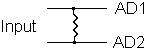
Q: "pulled up": What does this mean
Electronically/Electrically?
Q: What are buffers?
Q: So..., when we say (in
programming/SoftWare) that there is something in a Buffer...: what does
this mean Electronically? (from your explanation above)
Q: Are the switches Physical or just an
Abstract concept?
Q: Well, by saying "switch inputs" do you mean
that
Q: I have a question. I am currently working
on the 64 switch matrix program and circuit. I intend on using dip
switches for the matrix. My question is should I be concerned about the
ability of the 8255 to sink current when a large number of the switches
will be closed simultaneously. Is there a possibility of stressing the
device under the circumstances I have mentioned?
You are checking rows by taking bits from Port A low. It is possible
to connect one line of A to another one of its other lines by turning on
two switches at once. If you have taken one of them low, the other will
be high, causing them to "fight" each other and possibly stress the IC
beyond normal limits. As it stands, the circuit will permit only one
switch at a time to be turned on.
Experiment 4 will address this problem by placing diodes at each
cross-point.
Q: i just happened to surf on some reseach
related to my project and i found that your page provided me with more
than sufficient information.Its really awesome.By the way there is a
topic about how to use digital inputs to control motors....i would like
to ask you when will that information be released.By the way keep up the
good work!
Q: I'm really impressed by your description of
this I/O card. It has made me choose as a project for my summer study.
Since I stay in India, it won't be possible to meet you personally but I
hope to get a good support from you through emails. I would be grateful
to you if you could clarify a few points. The circuit is a bit complex.
I find it difficult to understand the different parts of the card. Can
you provide a block diagram ? Also, since I live far away from US, it
won't be feasible to buy the stuff from here. It would be very kind of
you if you could provide me with the PCB Layout.
Q: I wonder if you could send me an more
elaborative text/article (with programms) about INTERRUPTS: i.e. how the
whole mechanism works LOGICALLY... Thanks!
It's all interesing stuff, but not yet pertaining to my site. When I
do get into interrupts I'll cover some of the following. Meanwhile,
whoever sent this might consider asking the following questions of the
folks at the above URL since they wrote the article from which the
questions derive:
To hook an interrupt, a program need only to replace a specific
interrupt table entry with the address of its own interrupt handler.
Whenever this interrupt occurs, the handler is automatically invoked by
the processor. A good programming practice is to place a call to the
previous handler inside the interrupt handling function. This ensures
that all previously installed hooks will get a chance to handle the
incoming interrupt.
address of its own interrupt handler:
A good programming practice is to place a call to the previous
handler inside the interrupt handling function. This ensures that all
previously installed hooks will get a chance to handle the incoming
interrupt:
Note that when loading an application which uses software interrupts
to call operating system services, there is no need to patch the
application code with the actual memory addresses of the OS services.
Therefore, the operating system can freely relocate its services in
memory by simply updating the corresponding interrupt table entries with
the new addresses.
no need to patch the application code with the actual memory addresses of
the OS services:
What do you mean by PATCH?
operating system can freely relocate its services in memory:
A:You should be able to make a console
application, providing you can have direct port access. NT, 2000 and
others do not permit it.
and _outp, _outpw and _outpd
in VC++ help.
A:From what I have seen, it's experience or
degree, but you get a little edge with the paper. I have a degree in
Sociology with a minor in Psychology. That and a buck will get you a cup
of coffee unless they find out you are a sociologist -- then they charge
2 bucks. I went back and got a CS, going in the evenings after work.
Took 6 years but it was worth it.
Your tutorial is one of the best ones I have seen on the net. It
presents a very good entry level introduction for beginners like me.
Had a question or two for you. I am looking into making a
seismograph recorder using the Super Start board and I noticed on one of
your programs you have an oscilloscope program and I am thinking about
using the scope as the reader but I wanted to make some modifications to
it (Scan rate ect.) and I was wondering where the source code is or if
it is available? The other question is, do you have any plans to add
information on how to bit bang data on the tutorials?
A:For those who don't know, the board was
originally designed for The Super Start Project, which is where it gets
its name. Go to the QuickStart section of The Super Start Project at http://www.superstart.
org/quickstart.htm. You can download everything there in a zip file.
One of the sources is an assembly file. That's where a lot of the
recording code is. See the recplay.c file, about line 971, for the scope
routine. Also for those who haven't encountered it, bit banging is used
when you don't have a serial port available that's suitable for the type
of communication you need to do. Under such circumstances, a device such
as the PPI might be used to assemble a stream of bits in a manner
similar to a standard serial interface. I might be able to get into some
of that when I discuss timer interrupts.
A:Maybe one of the newsgroups such as those
listed at http://www.inprise.com/delphi/newsgroups will have the answer.
You might give them this site as an example of what you are trying to
do. Be sure you tell them the operating system you are running under.
You can't, for example, run some of the examples in the tutorial under
the NT operating system because it does not permit direct port access.
A: The clock is on B30. I left it out
before. Now it's included. Thank you.
A: Unlike outputs, inputs to some ICs float,
which is to say you can't count on them to be high or low. It's very
common to use resistors to pull them up to high logic, which is 5 volts
in this system. It's just as possible to have a pull down resistor to
ground. I'll get into that more in a latter experiment.
A: Buffers are used to increase the output
drive capability of a line, or to lighten the load seen by outside
circuits. This is sometimes called repowering. Some buffers have a third
line entering the side of the triangle. When it is not activated, the
output of the buffer is removed from the circuit to keep it from
interfering with other devices.
A: If I am understanding this correctly, I
would use IC7, the 74LS244, as an example. It has 3 inputs called
SWITCHIN1 2 and 3. It is possible to read this buffer programmatically,
and it is common to say they are "in" the buffer. When one is turned on,
its normally pulled-up input is pulled down to ground. That information
is considered in the buffer and can be read out of it.
A: These are just inputs (see above). A
better phrase might be "The switch inputs are designated SWITCHIN1,
SWITCHIN2 and SWITCHIN3 on the schematic and can be accessed on pins 5,
4 and 3 respectively of HEADER 1." (as a matter of fact, it is now)
1: That there is an INPUT
2: This INPUT acts as a SWITCH
OR a place where I can (Electrically/Electronically) connect
(i.e. wiring) a SWITCH-device...
or...?
A: All of the above, but the most accurate
would be that it is a place where a closure device can be connected.
A: I am going to get into more matrix
information in experiment 4. Please note what can happen if you close
two switches at once:
|-----------------------|
Port A bit 0| 4| 5| 6| 7| 8| 9|10|11|
Port A bit 1|12|13|14|15|16|17|18|19|
Port A bit 2|20|21|22|23|24|25|26|27|
Port A bit 3|28|29|30|31|32|33|34|35|
Port A bit 4|36|37|38|39|40|41|42|43|
Port A bit 5|44|45|46|47|48|49|50|51|
Port A bit 6|52|53|54|55|56|57|58|59|
Port A bit 7|60|61|62|63|64|65|66|67|
|-----------------------|
Port B bits 0 1 2 3 4 5 6 7
A:Soon and very soon (if you know the
reference). I hope to get into outputs in experiment 4. Actually, the
matrix in 3 uses A as an output and shows how to set up the 8255 for
output. Motors will probably be in 5 or 6.
A: The block diagram is a good idea, and I'm
working on it. In addition to copyright problems however, I don't have a
layout that could be used to make a board. I have the original films of
course, but obviously can't let them go!
A: This subject has yet to be covered. I
don't recall who sent this, but apparently the following questions
derive from the URL that was also in the message:
http://www.internals.com/articles_main.htm
hook an interrupt:
How does a code for HOOKING an interrrupt look like in Assembler and
C languanges?
How do you know the address of the Application's interrupt handler?
Don't you think that this will cause some conflict, I mean if the
handlers do different things...
Why will the OS need to relocate its services?